Latch up refers to a short circuit formed between power and ground pin in an IC leading to high current and damage to the IC. In CMOS transistor latch up is the phenomenon of low impedance path between power pin and ground pin due to interaction between parasitic PNP and NPN transistors. The structure formed by these resembles a Silicon Controlled rectifier(SCR). These form a positive feedback loop, short circuit the power and ground pin which eventually causes excessive current and can even permanently damage the device. Although the use of an epitaxial layer and other process improvements have lessened the severity of Latch Up problems but there is always a reliability concern for Latch Up, especially in I/O circuits.
The Latch Up susceptibility is inversely proportional to the product of the substrate doping level and the square of the spacing. In other words, if the spacing is reduced by half and the substrate doping is increased by two times, then the Latch Up susceptibility would increase by a factor of two.
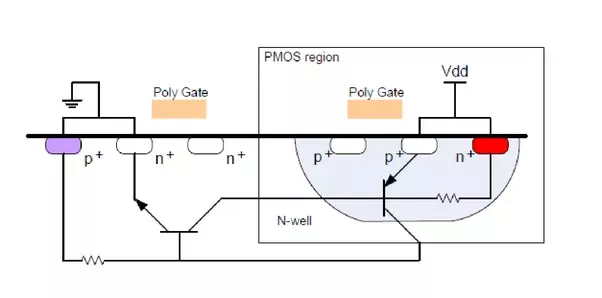
In the equivalent circuit, collector current of one transistor Q1 with it’s base to collector gain (β1) is fed as input base current to another transistor Q2 with it’s base to collector gain (β2). And this collector current Ic2 is fed as input base current Ib1 to another transistor Q1. In this way both transistors feedback each other and the collector current of each goes on multiplying by (β1*β2). This event is called the triggering of the SCR. Once triggered, each transistor drives the another transistor with positive feedback, eventually creating a low impedance path between the power and ground rails, resulting in Latch Up. It can be seen if the condition
β1*β2 ≥ 1
is satisfied. Now, both transistors will continue to conduct a high (saturation) current even after the triggering is no longer available. This latch up condition can also be written in terms of the collector-emitter gain as follows:
α1 + α2 ≥ 1
Latch up prevention Techniques:-
Latch up prevention includes putting a high resistance in path so as to limit the current through supply and make β1β2<1. This can be done with the help of following techniques:
- Surrounding PMOS and NMOS transistors with an insulating oxide layer.
- Latch up protection technology circuitry which shuts off the device when latch up is detected.
- Use minimum area p-wells (in case of twin-tub technology or n-type substrate) so that the p-well photocurrent can be minimized during transient pulses.
- Lay out n- and p-channel transistors such that all NMOS transistors are placed close to Vss and PMOS transistors are placed closed to Vdd lines. Also maintain sufficient spacings between PMOS and NMOS transistors.
Latest Post
Crosstalk is a phenomenon in which switching on a signal net affects switching activity of a nearby net due to capacitive coupling between two nets…