In VLSI sub-micron technology, due to scaling process the chip density is increasing day by day and respectively size of the transistors are reducing. The spaces between the wires are also decreasing and this causes many problems like short channel effect, signal crosstalk, heating problem etc.
Signal Crosstalk is a phenomenon in which the switching activity of a net wire affects the switching activity of its nearby wire because of coupling capacitance and inductance between the two nets. Crosstalk creates an undesired effect on the neighboring circuit or net which can affect the timing behavior of circuit or it can change the value of the signal voltage. For better understanding we divide Crosstalk into two parts.
- Crosstalk Noise Analysis:
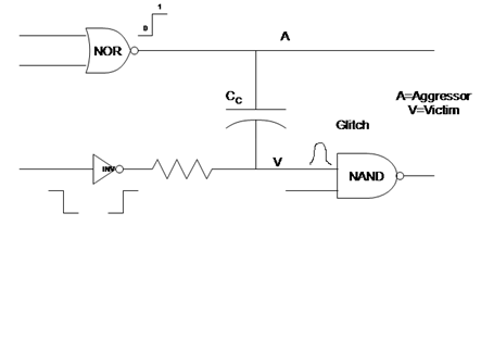
Lets consider the figure given below.

Consider there are two nets. One is aggressor (A) and another is victim (v). When the output of NOR gate is changed from 0 to 1, it can create a disturbance at V due to mutual coupling capacitance. If this glitch is strong enough, then it can change the input value of NAND gate, which will result in undesired output value.
2. Crosstalk Delay Analysis:
Crosstalk delay is same as crosstalk noise. The difference is that in crosstalk noise, one of the net is in steady mode but in crosstalk delay; both the nets are in active mode. The switching activity of victim and aggressor net result in the change of timing of a particular signal. When the two wires are switching in same direction, then it will add timing and if the both wires are switching in opposite direction, it will slow down the signal and results in setup violation.
Now consider the same example,
Suppose output of NOR gate is switching from logic ‘0 ’to logic‘1’ and at the same time, the output of inverter is switching from logic ‘1’ to logic 0’. Now, due to capacitive coupling, there will be a change in timing of victim net and it will be increased by a delay of ‘dt’. This will increase the total propagation delay of the circuit and affect the timing behavior.
The pulse width of the victim net will depend upon the net transition of aggressor. It means more rising and falling period of aggressor is sharp i.e. almost perpendicular, the shorter will be the pulse.
- Crosstalk due to inductance:
Till now, we only discussed crosstalk due to coupling capacitance, but inductive coupling is also responsible for crosstalk. Every wire has some intrinsic inductance. When the value of mutual inductance will be more than the value of intrinsic inductance, more will be the magnitude of the induced noise. Same case is also valid for capacitance. As the chip density increases, the problem of coupling capacitance and inductance also increases because the intrinsic capacitance becomes smaller. As capacitance and inductance of a wire depend upon its length, the crosstalk voltage is almost proportional to the coupling wire length.
- Methods for avoiding Crosstalk:
There are many ways for minimizing crosstalk. Some existing methods are:
- Wire spacing: As we increase the space between the neighboring wires, the coupling capacitance reduces and so as the crosstalk. It will also improve the circuit timing and power consumption. However, it will increase the total chip area.
- Shielding: Shielding means inserting the VDD or GND track between the two signal wires. However, coupling capacitance will not reduce in this case but it will eliminate neighboring switching explicitly.
- Buffer insertion and buffer sizing: Buffer increases the strength of victim signal. It strong the driving capabilities of net and reduces the interconnect delay.
- Using the minimum data rate and circuit bandwidth: Since the coupling capacitance directly depends on the rise time of the aggressor signal. If we reduce the signal circuit B.W. and minimize the required data rate, the coupling capacitance will also reduce and hence reducing the crosstalk.
Latest Post
Latch up refers to a short circuit formed between power and ground pin in an IC leading to high current and damage to the IC. In CMOS transistor latch up…
some genuinely great info , Gladiolus I found this.